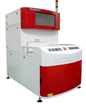
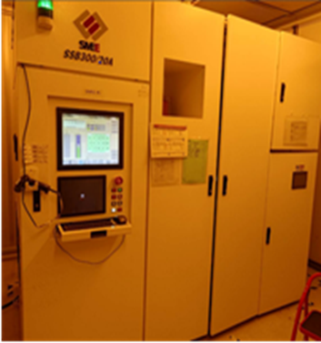
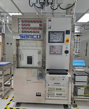
Manufacturing Process

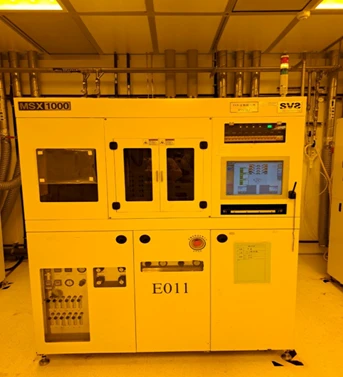
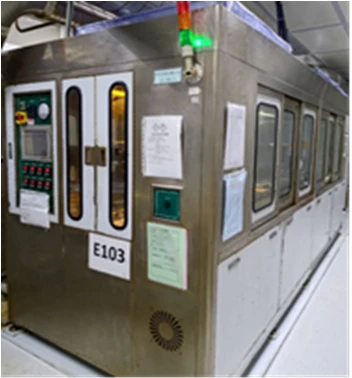
Manufacturing Process
Excellent thickness uniformity (<3%)
Maximum heating temperature ~350℃
Good temperature uniformity
Reflectivity can reach over 99%
Dense film layers, no spectral shift in coverage area
Spectral uniformity ≦±1%
Capable of low-temperature processing
Excellent thickness uniformity (<1%)
Optimal film density and adhesion
Lower deposition temperature
Adjustable film internal stress
Good step coverage capability
High-quality dense film
Fast heating rate (20℃/sec)
Maximum heating temperature ~900℃
Excellent temperature uniformity (Substrate ΔT <3℃)
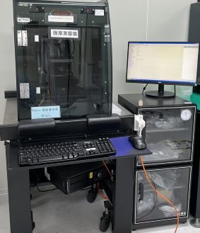
Advantages of stylus thickness measurement
Surface roughness and profile measurement
High stability and easy to operate
Adjustable variable temperature hotplate
Good coating uniformity (~1% internal/external)
Automated simultaneous processing of multiple photoresists
Resolution ~3μm
High-precision alignment system
High throughput and machine stability
Lower mask costs
Higher resolution ~1μm
High-precision alignment system
Superior machine stability
Adjustable variable temperature hotplate
Good development uniformity (~1% internal/external)
Combined physical and chemical etching
(Excellent etching directionality control)
Fully automated operating system
Automatic chemical supply system
High equipment stability
Superior wafer surface cleaning capability
Low ion energy to prevent chip damage